-
Part Symbol
-
Footprint
-
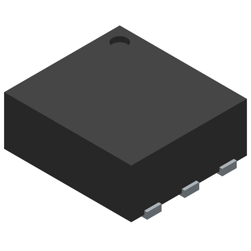
3D Model
Available Download Formats
By downloading CAD models, you agree to our Terms & Conditions and Privacy Policy
3A Ultra-Small Low Ron and Controlled Load Switch with Auto-Discharge Path, DFNW-6, 3000-REEL, Automotive Qualified
Tip: Data for a part may vary between manufacturers. You can filter for manufacturers on the top of the page next to the part image and part number.
NCV451AMNWTBG by onsemi is a Peripheral Driver.
Peripheral Drivers are under the broader part category of Drivers And Interfaces.
A driver controls the current or voltage delivered to components like LCDs or motors, while an interface component connects systems for data transfer and control. Read more about Drivers And Interfaces on our Drivers And Interfaces part category page.
| Part # | Distributor | Description | Stock | Price | Buy | |
|---|---|---|---|---|---|---|
|
DISTI #
85AC3012
|
Newark | 3A Ultra-Smallloadswitch/ Reel |Onsemi NCV451AMNWTBG RoHS: Not Compliant Min Qty: 3000 Package Multiple: 1 Date Code: 0 Container: Reel | 0 |
|
$0.3720 / $0.4840 | Buy Now |
|
DISTI #
488-NCV451AMNWTBGCT-ND
|
DigiKey | IC PWR SWITCH N-CHANNEL 1:1 6DFN Min Qty: 1 Lead time: 18 Weeks Container: Digi-Reel®, Cut Tape (CT), Tape & Reel (TR) |
3255 In Stock |
|
$0.3600 / $1.6200 | Buy Now |
|
DISTI #
NCV451AMNWTBG
|
Avnet Americas | Single Channel High Side Driver, 1 Channel, 5.5 V, 3 A, 45 Milliohms, 6 Pins, WDFN-EP - Tape and Ree... more RoHS: Compliant Min Qty: 3000 Package Multiple: 3000 Lead time: 18 Weeks, 0 Days Container: Reel |
6000 |
|
$0.3542 / $0.3888 | Buy Now |
|
DISTI #
863-NCV451AMNWTBG
|
Mouser Electronics | Power Switch ICs - Power Distribution 3A Ultra-Small Low Ron and Controlled Load Switch with Auto-Di... more RoHS: Compliant | 2412 |
|
$0.3600 / $1.5700 | Buy Now |
|
|
Onlinecomponents.com | 3A Ultra-Small Low Ron and Controlled Load Switch with Auto-Discharge Path RoHS: Compliant | 0 |
|
$0.3510 / $0.4110 | Buy Now |
|
DISTI #
86012897
|
Verical | Power Switch Hi Side 1-OUT 25Ohm 6-Pin DFNW EP T/R Automotive AEC-Q100 RoHS: Compliant Min Qty: 834 Package Multiple: 1 Date Code: 2201 | Americas - 48000 |
|
$0.4250 / $0.4500 | Buy Now |
|
|
Rochester Electronics | NCV451 - 3A Ultra-Small Low Ron and Controlled Load Switch with Auto-Discharge Path RoHS: Compliant Status: Active Min Qty: 1 | 48000 |
|
$0.3400 / $0.4000 | Buy Now |
|
|
Chip 1 Exchange | INSTOCK | 7718 |
|
RFQ | |
|
DISTI #
NCV451AMNWTBG
|
Avnet Silica | Single Channel High Side Driver 1 Channel 55 V 3 A 45 Milliohms 6 Pins WDFNEP (Alt: NCV451AMNWTBG) RoHS: Compliant Min Qty: 3000 Package Multiple: 3000 Lead time: 19 Weeks, 0 Days | Silica - 0 |
|
Buy Now | |
|
DISTI #
NCV451AMNWTBG
|
EBV Elektronik | Single Channel High Side Driver 1 Channel 55 V 3 A 45 Milliohms 6 Pins WDFNEP (Alt: NCV451AMNWTBG) RoHS: Compliant Min Qty: 3000 Package Multiple: 3000 Lead time: 20 Weeks, 0 Days | EBV - 0 |
|
Buy Now |
By downloading CAD models, you agree to our Terms & Conditions and Privacy Policy
|
|
NCV451AMNWTBG
onsemi
Buy Now
Datasheet
|
Compare Parts:
NCV451AMNWTBG
onsemi
3A Ultra-Small Low Ron and Controlled Load Switch with Auto-Discharge Path, DFNW-6, 3000-REEL, Automotive Qualified
Select a part to compare: |
| Pbfree Code | Yes | |
| Rohs Code | Yes | |
| Part Life Cycle Code | Active | |
| Ihs Manufacturer | ONSEMI | |
| Part Package Code | DFNW-6 | |
| Package Description | DFN-6 | |
| Manufacturer Package Code | 507AF | |
| Reach Compliance Code | compliant | |
| ECCN Code | EAR99 | |
| HTS Code | 8542.39.00.01 | |
| Factory Lead Time | 18 Weeks | |
| Samacsys Manufacturer | onsemi | |
| Built-in Protections | TRANSIENT | |
| Interface IC Type | BUFFER OR INVERTER BASED PERIPHERAL DRIVER | |
| JESD-30 Code | R-PDSO-N6 | |
| JESD-609 Code | e3 | |
| Length | 2.2 mm | |
| Moisture Sensitivity Level | 1 | |
| Number of Functions | 1 | |
| Number of Terminals | 6 | |
| Operating Temperature-Max | 105 °C | |
| Operating Temperature-Min | -40 °C | |
| Output Current Flow Direction | SINK | |
| Package Body Material | PLASTIC/EPOXY | |
| Package Code | HVSON | |
| Package Shape | RECTANGULAR | |
| Package Style | SMALL OUTLINE, HEAT SINK/SLUG, VERY THIN PROFILE | |
| Peak Reflow Temperature (Cel) | 260 | |
| Seated Height-Max | 0.9 mm | |
| Supply Voltage-Max | 5.5 V | |
| Supply Voltage-Min | 0.75 V | |
| Supply Voltage-Nom | 3.6 V | |
| Surface Mount | YES | |
| Temperature Grade | INDUSTRIAL | |
| Terminal Finish | MATTE TIN | |
| Terminal Form | NO LEAD | |
| Terminal Pitch | 0.65 mm | |
| Terminal Position | DUAL | |
| Time@Peak Reflow Temperature-Max (s) | 30 | |
| Width | 2 mm |