-
Part Symbol
-
Footprint
-
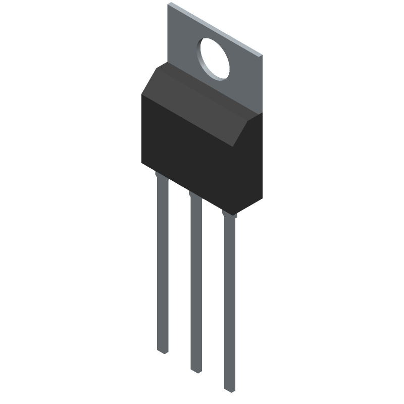
3D Model
Available Download Formats
By downloading CAD models, you agree to our Terms & Conditions and Privacy Policy
25 A, 100 V NPN Bipolar Power Transistor, SOT-93 (T0-218) 4 LEAD, 30-TUBE
Tip: Data for a part may vary between manufacturers. You can filter for manufacturers on the top of the page next to the part image and part number.
TIP35C by onsemi is a Power Bipolar Transistor.
Power Bipolar Transistors are under the broader part category of Transistors.
A transistor is a small semiconductor device used to amplify, control, or create electrical signals. When selecting a transistor, factors such as voltage, current rating, gain, and power dissipation must be considered, with common types. Read more about Transistors on our Transistors part category page.
By downloading CAD models, you agree to our Terms & Conditions and Privacy Policy
|
|
TIP35C
onsemi
Buy Now
Datasheet
|
Compare Parts:
TIP35C
onsemi
25 A, 100 V NPN Bipolar Power Transistor, SOT-93 (T0-218) 4 LEAD, 30-TUBE
Select a part to compare: |
| Pbfree Code | No | |
| Rohs Code | No | |
| Part Life Cycle Code | Obsolete | |
| Ihs Manufacturer | ONSEMI | |
| Part Package Code | SOT-93 (T0-218) 4 LEAD | |
| Package Description | CASE 340D-02, 3 PIN | |
| Pin Count | 3 | |
| Manufacturer Package Code | 340D-02 | |
| Reach Compliance Code | not_compliant | |
| ECCN Code | EAR99 | |
| HTS Code | 8541.29.00.95 | |
| Samacsys Manufacturer | onsemi | |
| Case Connection | COLLECTOR | |
| Collector Current-Max (IC) | 25 A | |
| Collector-Emitter Voltage-Max | 100 V | |
| Configuration | SINGLE | |
| DC Current Gain-Min (hFE) | 15 | |
| JEDEC-95 Code | TO-218 | |
| JESD-30 Code | R-PSFM-T3 | |
| JESD-609 Code | e0 | |
| Number of Elements | 1 | |
| Number of Terminals | 3 | |
| Operating Temperature-Max | 150 °C | |
| Package Body Material | PLASTIC/EPOXY | |
| Package Shape | RECTANGULAR | |
| Package Style | FLANGE MOUNT | |
| Peak Reflow Temperature (Cel) | 235 | |
| Polarity/Channel Type | NPN | |
| Power Dissipation-Max (Abs) | 125 W | |
| Qualification Status | Not Qualified | |
| Surface Mount | NO | |
| Terminal Finish | Tin/Lead (Sn/Pb) | |
| Terminal Form | THROUGH-HOLE | |
| Terminal Position | SINGLE | |
| Time@Peak Reflow Temperature-Max (s) | 30 | |
| Transistor Application | SWITCHING | |
| Transistor Element Material | SILICON | |
| Transition Frequency-Nom (fT) | 3 MHz |
This table gives cross-reference parts and alternative options found for TIP35C. The Form Fit Function (FFF) tab will give you the options that are more likely to serve as direct pin-to-pin alternates or drop-in parts. The Functional Equivalents tab will give you options that are likely to match the same function of TIP35C, but it may not fit your design. Always verify details of parts you are evaluating, as these parts are offered as suggestions for what you are looking for and are not guaranteed.
| Part Number | Manufacturer | Composite Price | Description | Compare |
|---|---|---|---|---|
| TIP35CG | onsemi | $2.0138 | 25 A, 100 V NPN Bipolar Power Transistor, TO-247, 30-TUBE | TIP35C vs TIP35CG |
The maximum safe operating temperature for the TIP35C is 150°C, as specified in the datasheet. However, it's recommended to operate the transistor at a temperature below 125°C for optimal performance and reliability.
To ensure the TIP35C is properly biased for linear operation, you should ensure that the base-emitter voltage (VBE) is between 0.6V to 0.8V, and the collector-emitter voltage (VCE) is at least 1V. Additionally, the base current should be limited to prevent overheating.
The maximum current handling capability of the TIP35C is 15A, as specified in the datasheet. However, it's recommended to derate the current handling capability based on the operating temperature and other environmental factors.
Yes, the TIP35C can be used as a switch, but it's essential to ensure that the transistor is fully saturated (VCE < 0.5V) to minimize power dissipation. Additionally, consider the switching frequency, as high-frequency switching can lead to increased power losses and reduced reliability.
To protect the TIP35C from electrical overstress (EOS), use a voltage clamp or a transient voltage suppressor (TVS) to limit the voltage across the transistor. Additionally, ensure that the transistor is properly biased and that the operating conditions are within the specified limits.