-
Part Symbol
-
Footprint
-
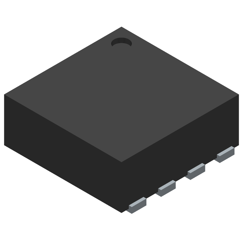
3D Model
Available Download Formats
By downloading CAD models, you agree to our Terms & Conditions and Privacy Policy
Ultra-Low-Noise, High PSRR, Low-Dropout, 120mA Linear Regulators, 8-LFCSP-2X2X0.75, 8 Pins, -40 to 85C
Tip: Data for a part may vary between manufacturers. You can filter for manufacturers on the top of the page next to the part image and part number.
MAX8510ETA33+T by Analog Devices Inc is a Linear Regulator IC.
Linear Regulator ICs are under the broader part category of Power Circuits.
A power circuit delivers electricity in order to operate a load for an electronic device. Power circuits include transformers, generators and switches. Read more about Power Circuits on our Power Circuits part category page.
| Part # | Distributor | Description | Stock | Price | Buy | |
|---|---|---|---|---|---|---|
|
DISTI #
700-MAX8510ETA33T
|
Mouser Electronics | LDO Voltage Regulators Ultra-Low-Noise, High PSRR, Low-Dropout, RoHS: Compliant | 194 |
|
$0.9090 / $2.9400 | Buy Now |
|
|
Analog Devices Inc | Ultra-Low-Noise, High PSRR, Lo Min Qty: 2500 Package Multiple: 1 | 37500 |
|
$0.7000 / $0.8750 | Buy Now |
By downloading CAD models, you agree to our Terms & Conditions and Privacy Policy
|
|
MAX8510ETA33+T
Analog Devices Inc
Buy Now
Datasheet
|
Compare Parts:
MAX8510ETA33+T
Analog Devices Inc
Ultra-Low-Noise, High PSRR, Low-Dropout, 120mA Linear Regulators, 8-LFCSP-2X2X0.75, 8 Pins, -40 to 85C
Select a part to compare: |
| Rohs Code | Yes | |
| Part Life Cycle Code | Active | |
| Ihs Manufacturer | ANALOG DEVICES INC | |
| Part Package Code | 8-LFCSP-2X2X0.75 | |
| Pin Count | 8 | |
| Manufacturer Package Code | 8-LFCSP-2X2X0.75 | |
| Reach Compliance Code | compliant | |
| Date Of Intro | 2003-02-26 | |
| Samacsys Manufacturer | Analog Devices | |
| Adjustability | FIXED | |
| Dropout Voltage1-Max | 0.17 V | |
| Dropout Voltage1-Nom | 0.12 V | |
| Input Voltage Absolute-Max | 7 V | |
| Input Voltage-Max | 6 V | |
| Input Voltage-Min | 2 V | |
| JESD-30 Code | S-XDSO-N8 | |
| JESD-609 Code | e3 | |
| Length | 2 mm | |
| Moisture Sensitivity Level | 1 | |
| Number of Functions | 1 | |
| Number of Outputs | 1 | |
| Number of Terminals | 8 | |
| Operating Temperature TJ-Max | 150 °C | |
| Output Current1-Max | 0.12 A | |
| Output Voltage1-Max | 3.399 V | |
| Output Voltage1-Min | 3.201 V | |
| Output Voltage1-Nom | 3.3 V | |
| Package Body Material | UNSPECIFIED | |
| Package Code | HVSON | |
| Package Equivalence Code | SOLCC8,.08,20 | |
| Package Shape | SQUARE | |
| Package Style | SMALL OUTLINE, HEAT SINK/SLUG, VERY THIN PROFILE | |
| Packing Method | TR | |
| Peak Reflow Temperature (Cel) | 260 | |
| Qualification Status | Not Qualified | |
| Regulator Type | FIXED POSITIVE SINGLE OUTPUT LDO REGULATOR | |
| Seated Height-Max | 0.8 mm | |
| Surface Mount | YES | |
| Technology | BICMOS | |
| Terminal Finish | Matte Tin (Sn) | |
| Terminal Form | NO LEAD | |
| Terminal Pitch | 0.5 mm | |
| Terminal Position | DUAL | |
| Time@Peak Reflow Temperature-Max (s) | 30 | |
| Voltage Tolerance-Max | 3% | |
| Width | 2 mm |
This table gives cross-reference parts and alternative options found for MAX8510ETA33+T. The Form Fit Function (FFF) tab will give you the options that are more likely to serve as direct pin-to-pin alternates or drop-in parts. The Functional Equivalents tab will give you options that are likely to match the same function of MAX8510ETA33+T, but it may not fit your design. Always verify details of parts you are evaluating, as these parts are offered as suggestions for what you are looking for and are not guaranteed.
| Part Number | Manufacturer | Composite Price | Description | Compare |
|---|---|---|---|---|
| MAX8510ETA33+T | Maxim Integrated Products | Check for Price | Fixed Positive LDO Regulator, 3.3V, 0.17V Dropout, BICMOS, 2 X 2 MM, 0.80 MM HEIGHT, LEAD FREE, MO-229, TDFN-8 | MAX8510ETA33+T vs MAX8510ETA33+T |
| MAX8511ETA33+T | Maxim Integrated Products | Check for Price | Fixed Positive LDO Regulator, 3.3V, 0.17V Dropout, BICMOS, 2 X 2 MM, 0.80 MM HEIGHT, LEAD FREE, MO-229, TDFN-8 | MAX8510ETA33+T vs MAX8511ETA33+T |
A good PCB layout for the MAX8510ETA33+T involves keeping the input and output traces short and separate, using a solid ground plane, and placing the device close to the power source. Additionally, it's recommended to use a 4-layer PCB with a dedicated power plane and a dedicated ground plane to minimize noise and EMI.
To ensure proper powering and decoupling of the MAX8510ETA33+T, use a high-quality, low-ESR capacitor (e.g., 10uF ceramic) between the VIN pin and GND, and a smaller capacitor (e.g., 100nF ceramic) between the VCC pin and GND. Place these capacitors as close to the device as possible.
The maximum allowed input voltage for the MAX8510ETA33+T is 6V. Exceeding this voltage may damage the device. It's recommended to use a voltage regulator or a voltage limiter to ensure the input voltage remains within the specified range.
To troubleshoot issues with the MAX8510ETA33+T, start by verifying the input voltage and current, and checking for proper decoupling and PCB layout. Use an oscilloscope to measure the output voltage and check for oscillations. Also, ensure that the device is properly soldered and that there are no shorts or opens on the PCB.
The MAX8510ETA33+T is rated for operation up to 125°C. However, the device's performance and reliability may degrade at high temperatures. It's recommended to derate the device's output current and voltage at high temperatures, and to ensure proper thermal management and heat sinking.