-
Part Symbol
-
Footprint
-
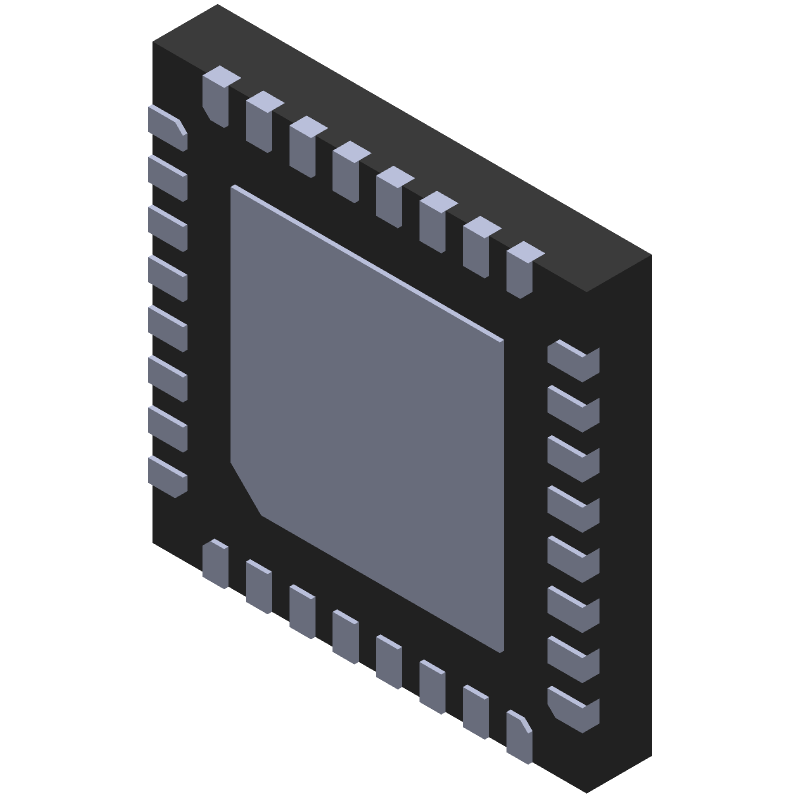
3D Model
Available Download Formats
By downloading CAD models, you agree to our Terms & Conditions and Privacy Policy
16-Bit, 6-Channel, 64ksps, 6.2nV/√Hz PGA, Delta-Sigma ADC with SPI Interface, 32-LFCSP-5X5X0.75, 32 Pins, -40 to 125C
Tip: Data for a part may vary between manufacturers. You can filter for manufacturers on the top of the page next to the part image and part number.
MAX11253ATJ+ by Analog Devices Inc is an Analog to Digital Converter.
Analog to Digital Converters are under the broader part category of Converters.
A converter is an electrical circuit that transforms electric energy into a different form that will support a elecrical load needed by a device. Read more about Converters on our Converters part category page.
| Part # | Distributor | Description | Stock | Price | Buy | |
|---|---|---|---|---|---|---|
|
DISTI #
700-MAX11253ATJ+
|
Mouser Electronics | Analog to Digital Converters - ADC 16-bit, 6-channel, 64ksps, integrated PG RoHS: Compliant | 113 |
|
$8.1000 / $15.3400 | Buy Now |
|
|
Analog Devices Inc | 16-bit, 6-channel, 64ksps, int Package Multiple: 1 | 1870 |
|
$6.4800 / $15.3400 | Buy Now |
|
|
Vyrian | Converters | 608 |
|
RFQ |
By downloading CAD models, you agree to our Terms & Conditions and Privacy Policy
|
|
MAX11253ATJ+
Analog Devices Inc
Buy Now
Datasheet
|
Compare Parts:
MAX11253ATJ+
Analog Devices Inc
16-Bit, 6-Channel, 64ksps, 6.2nV/√Hz PGA, Delta-Sigma ADC with SPI Interface, 32-LFCSP-5X5X0.75, 32 Pins, -40 to 125C
Select a part to compare: |
| Rohs Code | Yes | |
| Part Life Cycle Code | Active | |
| Ihs Manufacturer | ANALOG DEVICES INC | |
| Part Package Code | 32-LFCSP-5X5X0.75 | |
| Package Description | TQFN-32 | |
| Pin Count | 32 | |
| Manufacturer Package Code | 32-LFCSP-5X5X0.75 | |
| Reach Compliance Code | compliant | |
| Date Of Intro | 2015-08-20 | |
| Samacsys Manufacturer | Analog Devices | |
| Analog Input Voltage-Max | 3.6 V | |
| Analog Input Voltage-Min | -1.5 V | |
| Converter Type | ADC, DELTA-SIGMA | |
| JESD-30 Code | S-XQCC-N32 | |
| JESD-609 Code | e3 | |
| Length | 5 mm | |
| Linearity Error-Max (EL) | ||
| Moisture Sensitivity Level | 1 | |
| Negative Supply Voltage-Nom | ||
| Number of Analog In Channels | 6 | |
| Number of Bits | 16 | |
| Number of Functions | 1 | |
| Number of Terminals | 32 | |
| Operating Temperature-Max | 125 °C | |
| Operating Temperature-Min | -40 °C | |
| Output Bit Code | 2'S COMPLEMENT BINARY | |
| Output Format | SERIAL | |
| Package Body Material | UNSPECIFIED | |
| Package Code | HVQCCN | |
| Package Shape | SQUARE | |
| Package Style | CHIP CARRIER, HEAT SINK/SLUG, VERY THIN PROFILE | |
| Peak Reflow Temperature (Cel) | 260 | |
| Sample Rate | 0.064 MHz | |
| Seated Height-Max | 0.8 mm | |
| Supply Voltage-Nom | 3.6 V | |
| Surface Mount | YES | |
| Technology | CMOS | |
| Temperature Grade | AUTOMOTIVE | |
| Terminal Finish | Matte Tin (Sn) | |
| Terminal Form | NO LEAD | |
| Terminal Pitch | 0.5 mm | |
| Terminal Position | QUAD | |
| Time@Peak Reflow Temperature-Max (s) | 30 | |
| Width | 5 mm |