-
Part Symbol
-
Footprint
-
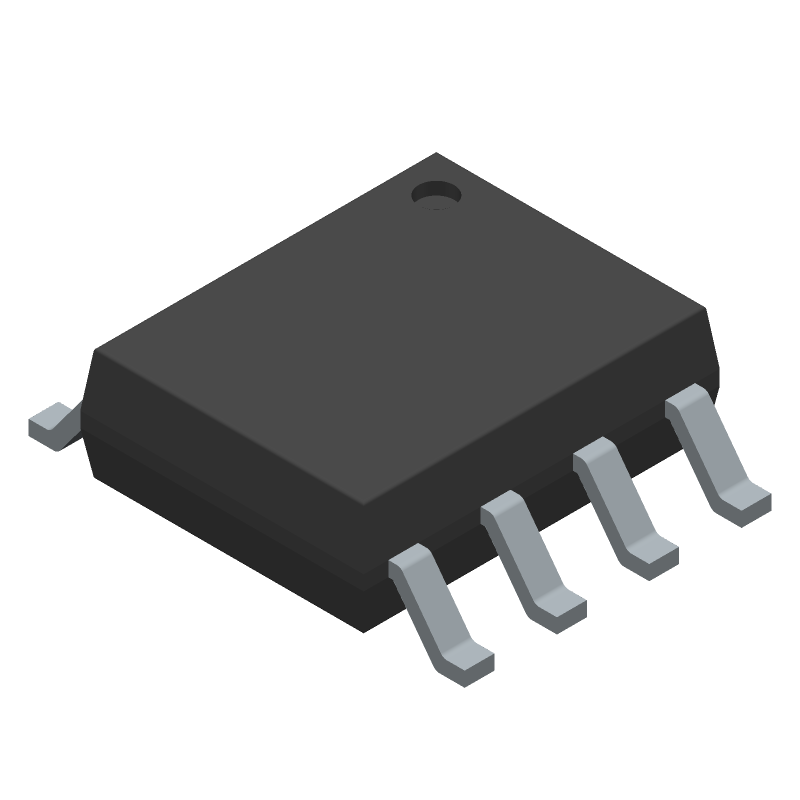
3D Model
Available Download Formats
By downloading CAD models, you agree to our Terms & Conditions and Privacy Policy
Analog Circuit, 1 Func, PDSO8, SOP-8/7
Tip: Data for a part may vary between manufacturers. You can filter for manufacturers on the top of the page next to the part image and part number.
LNK613DG by Power Integrations is an Other Signal Circuit.
Other Signal Circuits are under the broader part category of Signal Circuits.
A signal is an electronic means of transmitting information, either as an analog signal with continuous values or a digital signal with discrete values. Signals are used in various systems and networks. Read more about Signal Circuits on our Signal Circuits part category page.
| Part # | Distributor | Description | Stock | Price | Buy | |
|---|---|---|---|---|---|---|
|
DISTI #
596-1222-5-ND
|
DigiKey | IC OFFLINE SWITCH FLYBACK 8SO Lead time: 4 Weeks Container: Tube | Limited Supply - Call |
|
Buy Now | |
|
DISTI #
LNK613DG
|
EBV Elektronik | CVCC Switcher 7Pin SOICC (Alt: LNK613DG) RoHS: Compliant Min Qty: 100 Package Multiple: 100 | EBV - 0 |
|
Buy Now |
By downloading CAD models, you agree to our Terms & Conditions and Privacy Policy
|
|
LNK613DG
Power Integrations
Buy Now
Datasheet
|
Compare Parts:
LNK613DG
Power Integrations
Analog Circuit, 1 Func, PDSO8, SOP-8/7
Select a part to compare: |
| Rohs Code | Yes | |
| Part Life Cycle Code | Active | |
| Ihs Manufacturer | POWER INTEGRATIONS INC | |
| Part Package Code | SOIC | |
| Package Description | , | |
| Pin Count | 8 | |
| Reach Compliance Code | compliant | |
| ECCN Code | EAR99 | |
| HTS Code | 8542.39.00.01 | |
| Samacsys Manufacturer | Power Integrations |