-
Part Symbol
-
Footprint
-
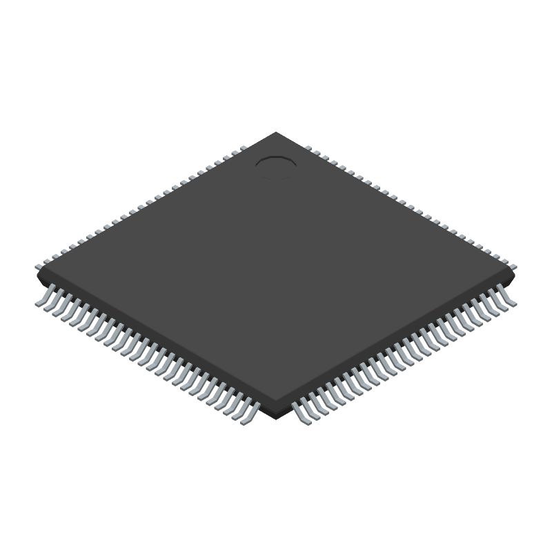
3D Model
Available Download Formats
By downloading CAD models, you agree to our Terms & Conditions and Privacy Policy
4 x 50 W PWM digital input power amplifier with built-in diagnostics features and low voltage operation
Tip: Data for a part may vary between manufacturers. You can filter for manufacturers on the top of the page next to the part image and part number.
| Part # | Distributor | Description | Stock | Price | Buy | |
|---|---|---|---|---|---|---|
|
DISTI #
FDA450LV
|
Avnet Americas | Audio Amp Speaker 4-CH Stereo 78W Class-D 100-Pin TQFP Tray - Trays (Alt: FDA450LV) RoHS: Compliant Min Qty: 540 Package Multiple: 540 Lead time: 111 Weeks, 0 Days Container: Tray | 0 |
|
RFQ | |
|
DISTI #
FDA450LV
|
Avnet Silica | Audio Amp Speaker 4CH Stereo 78W ClassD 100Pin TQFP Tray (Alt: FDA450LV) RoHS: Compliant Min Qty: 90 Package Multiple: 90 Lead time: 17 Weeks, 0 Days | Silica - 0 |
|
Buy Now | |
|
DISTI #
FDA450LV
|
EBV Elektronik | Audio Amp Speaker 4CH Stereo 78W ClassD 100Pin TQFP Tray (Alt: FDA450LV) RoHS: Compliant Min Qty: 90 Package Multiple: 90 Lead time: 143 Weeks, 0 Days | EBV - 0 |
|
Buy Now |
By downloading CAD models, you agree to our Terms & Conditions and Privacy Policy
|
|
FDA450LV
STMicroelectronics
Buy Now
Datasheet
|
Compare Parts:
FDA450LV
STMicroelectronics
4 x 50 W PWM digital input power amplifier with built-in diagnostics features and low voltage operation
Select a part to compare: |
| Rohs Code | Yes | |
| Part Life Cycle Code | Not Recommended | |
| Ihs Manufacturer | STMICROELECTRONICS | |
| Package Description | TQFP-100 | |
| Reach Compliance Code | compliant | |
| ECCN Code | EAR99 | |
| HTS Code | 8542.33.00.01 | |
| Factory Lead Time | 111 Weeks | |
| Samacsys Manufacturer | STMicroelectronics | |
| Consumer IC Type | CLASS D AUDIO AMPLIFIER | |
| Harmonic Distortion | 0.2% | |
| JESD-30 Code | S-PQFP-G100 | |
| Length | 14 mm | |
| Moisture Sensitivity Level | 3 | |
| Number of Channels | 4 | |
| Number of Functions | 1 | |
| Number of Terminals | 100 | |
| Operating Temperature-Max | 105 °C | |
| Operating Temperature-Min | -40 °C | |
| Output Power-Nom | 78 W | |
| Package Body Material | PLASTIC/EPOXY | |
| Package Code | HTFQFP | |
| Package Equivalence Code | TQFP100,.63SQ | |
| Package Shape | SQUARE | |
| Package Style | FLATPACK, HEAT SINK/SLUG, THIN PROFILE, FINE PITCH | |
| Peak Reflow Temperature (Cel) | NOT SPECIFIED | |
| Qualification Status | Not Qualified | |
| Seated Height-Max | 1.09 mm | |
| Supply Voltage-Max (Vsup) | 25 V | |
| Supply Voltage-Min (Vsup) | 6 V | |
| Surface Mount | YES | |
| Technology | BCDMOS | |
| Temperature Grade | INDUSTRIAL | |
| Terminal Form | GULL WING | |
| Terminal Pitch | 0.5 mm | |
| Terminal Position | QUAD | |
| Time@Peak Reflow Temperature-Max (s) | NOT SPECIFIED | |
| Width | 14 mm |
A good PCB layout for the FDA450LV involves keeping the analog and digital grounds separate, using a solid ground plane, and placing the device close to the analog signal sources to minimize noise. Additionally, it's recommended to use a 4-layer PCB with a dedicated power plane and a dedicated ground plane.
To ensure proper powering and decoupling of the FDA450LV, use a high-quality, low-ESR capacitor (e.g., 10uF) between the VCC and GND pins, and add a 100nF capacitor between the VCC and AVCC pins. Also, use a separate power supply for the analog and digital sections.
The recommended clock frequency for the FDA450LV is between 10 kHz and 100 kHz. However, the device can operate at frequencies up to 200 kHz, but with reduced performance and increased power consumption.
To optimize the FDA450LV for low-power operation, use the device's built-in power-down modes, reduce the clock frequency, and minimize the number of active channels. Additionally, consider using a lower supply voltage (e.g., 3.3V) and optimizing the external circuitry for low power consumption.
The FDA450LV can handle input signal amplitudes up to ±10V, but the maximum recommended amplitude is ±5V to ensure optimal performance and linearity.