-
Part Symbol
-
Footprint
-
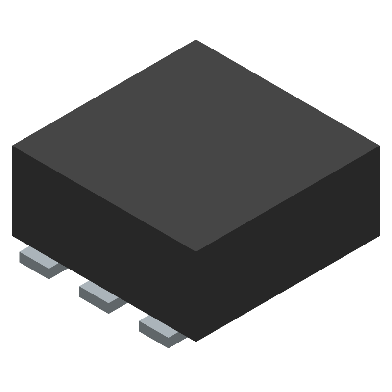
3D Model
Available Download Formats
By downloading CAD models, you agree to our Terms & Conditions and Privacy Policy

30-V, N channel NexFET™ power MOSFET, single SON 2 mm x 2 mm, 32 mOhm 6-WSON -55 to 150
Tip: Data for a part may vary between manufacturers. You can filter for manufacturers on the top of the page next to the part image and part number.
| Part # | Distributor | Description | Stock | Price | Buy | |
|---|---|---|---|---|---|---|
|
DISTI #
29AH3828
|
Newark | Mosfet, N Ch, 30V, 5A, Son-6, Transistor Polarity:N Channel, Continuous Drain Current Id:5A, Drain Source Voltage Vds:30V, On Resistance Rds(On):0.024Ohm, Rds(On) Test Voltage Vgs:8V, Threshold Voltage Vgs:1.3V, Power Dissipation Rohs Compliant: Yes |TEXAS INSTRUMENTS CSD17313Q2 Min Qty: 1 Package Multiple: 1 Date Code: 1 Container: Cut Tape | 12 |
|
$0.3720 / $0.4890 | Buy Now |
|
DISTI #
296-27233-1-ND
|
DigiKey | MOSFET N-CH 30V 5A 6WSON Min Qty: 1 Lead time: 6 Weeks Container: Cut Tape (CT), Digi-Reel®, Tape & Reel (TR) |
9265 In Stock |
|
$0.1373 / $0.4700 | Buy Now |
|
DISTI #
595-CSD17313Q2
|
Mouser Electronics | MOSFET 30V N Channel NexFET Power MOSFET RoHS: Compliant | 43097 |
|
$0.1370 / $0.4700 | Buy Now |
|
|
Bristol Electronics | Min Qty: 12 | 275 |
|
$0.1688 / $0.4500 | Buy Now |
|
|
Quest Components | 5 A, 30 V, 0.042 ohm, N-CHANNEL, Si, POWER, MOSFET | 220 |
|
$0.1800 / $0.6000 | Buy Now |
|
|
Quest Components | 5 A, 30 V, 0.042 ohm, N-CHANNEL, Si, POWER, MOSFET | 77 |
|
$0.7333 / $1.4665 | Buy Now |
|
|
Ameya Holding Limited | MOSFET N-CH 30V 5A 6SON | 33 |
|
RFQ | |
|
|
Component Electronics, Inc | IN STOCK SHIP TODAY | 2066 |
|
$0.3500 / $0.5400 | Buy Now |
|
|
Win Source Electronics | Trans MOSFET N-CH Si 30V 7.3A 6-Pin WSON EP T/R / MOSFET N-CH 30V 5A | 230000 |
|
$0.2910 / $0.4370 | Buy Now |
By downloading CAD models, you agree to our Terms & Conditions and Privacy Policy
|
|
CSD17313Q2
Texas Instruments
Buy Now
Datasheet
|
Compare Parts:
CSD17313Q2
Texas Instruments
30-V, N channel NexFET™ power MOSFET, single SON 2 mm x 2 mm, 32 mOhm 6-WSON -55 to 150
|
| Pbfree Code | Yes | |
| Rohs Code | Yes | |
| Part Life Cycle Code | Active | |
| Ihs Manufacturer | TEXAS INSTRUMENTS INC | |
| Package Description | SON-8 | |
| Pin Count | 8 | |
| Reach Compliance Code | compliant | |
| ECCN Code | EAR99 | |
| HTS Code | 8541.29.00.95 | |
| Samacsys Manufacturer | Texas Instruments | |
| Avalanche Energy Rating (Eas) | 18 mJ | |
| Case Connection | DRAIN | |
| Configuration | SINGLE WITH BUILT-IN DIODE | |
| DS Breakdown Voltage-Min | 30 V | |
| Drain Current-Max (ID) | 5 A | |
| Drain-source On Resistance-Max | 0.042 Ω | |
| FET Technology | METAL-OXIDE SEMICONDUCTOR | |
| Feedback Cap-Max (Crss) | 17 pF | |
| JESD-30 Code | R-PDSO-N8 | |
| JESD-609 Code | e4 | |
| Moisture Sensitivity Level | 1 | |
| Number of Elements | 1 | |
| Number of Terminals | 8 | |
| Operating Mode | ENHANCEMENT MODE | |
| Operating Temperature-Max | 150 °C | |
| Operating Temperature-Min | -55 °C | |
| Package Body Material | PLASTIC/EPOXY | |
| Package Shape | RECTANGULAR | |
| Package Style | SMALL OUTLINE | |
| Peak Reflow Temperature (Cel) | 260 | |
| Polarity/Channel Type | N-CHANNEL | |
| Power Dissipation-Max (Abs) | 17 W | |
| Pulsed Drain Current-Max (IDM) | 20 A | |
| Qualification Status | Not Qualified | |
| Surface Mount | YES | |
| Terminal Finish | NICKEL PALLADIUM GOLD | |
| Terminal Form | NO LEAD | |
| Terminal Position | DUAL | |
| Time@Peak Reflow Temperature-Max (s) | 30 | |
| Transistor Application | SWITCHING | |
| Transistor Element Material | SILICON |
This table gives cross-reference parts and alternative options found for CSD17313Q2. The Form Fit Function (FFF) tab will give you the options that are more likely to serve as direct pin-to-pin alternates or drop-in parts. The Functional Equivalents tab will give you options that are likely to match the same function of CSD17313Q2, but it may not fit your design. Always verify details of parts you are evaluating, as these parts are offered as suggestions for what you are looking for and are not guaranteed.
| Part Number | Description | Manufacturer | Compare |
|---|---|---|---|
| CSD17313Q2Q1 | Automotive 30-V N channel NexFET™ power MOSFET 6-WSON -55 to 150 | Texas Instruments | CSD17313Q2 vs CSD17313Q2Q1 |
| CSD17313Q2T | 30-V, N channel NexFET™ power MOSFET, single SON 2 mm x 2 mm, 32 mOhm 6-WSON -55 to 150 | Texas Instruments | CSD17313Q2 vs CSD17313Q2T |