-
Part Symbol
-
Footprint
-
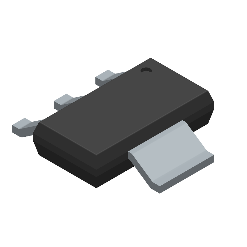
3D Model
Available Download Formats
By downloading CAD models, you agree to our Terms & Conditions and Privacy Policy
Power Field-Effect Transistor, 0.19A I(D), 800V, 20ohm, 1-Element, N-Channel, Silicon, Metal-oxide Semiconductor FET, GREEN, PLASTIC PACKAGE-4
Tip: Data for a part may vary between manufacturers. You can filter for manufacturers on the top of the page next to the part image and part number.
BSP300H6327XUSA1 by Infineon Technologies AG is a Power Field-Effect Transistor.
Power Field-Effect Transistors are under the broader part category of Transistors.
A transistor is a small semiconductor device used to amplify, control, or create electrical signals. When selecting a transistor, factors such as voltage, current rating, gain, and power dissipation must be considered, with common types. Read more about Transistors on our Transistors part category page.
| Part # | Distributor | Description | Stock | Price | Buy | |
|---|---|---|---|---|---|---|
|
DISTI #
SP001058720
|
EBV Elektronik | Trans MOSFET NCH 800V 019A 4Pin SOT223 TR (Alt: SP001058720) RoHS: Compliant Min Qty: 1000 Package Multiple: 1000 Lead time: 143 Weeks, 0 Days | EBV - 0 |
|
Buy Now | |
|
|
Vyrian | Transistors | 1595 |
|
RFQ | |
|
|
Win Source Electronics | MOSFET N-CH 800V 190MA SOT-223 | 16900 |
|
$0.9661 / $1.4491 | Buy Now |
By downloading CAD models, you agree to our Terms & Conditions and Privacy Policy
|
|
BSP300H6327XUSA1
Infineon Technologies AG
Buy Now
Datasheet
|
Compare Parts:
BSP300H6327XUSA1
Infineon Technologies AG
Power Field-Effect Transistor, 0.19A I(D), 800V, 20ohm, 1-Element, N-Channel, Silicon, Metal-oxide Semiconductor FET, GREEN, PLASTIC PACKAGE-4
Select a part to compare: |
| Pbfree Code | Yes | |
| Rohs Code | Yes | |
| Part Life Cycle Code | Obsolete | |
| Ihs Manufacturer | INFINEON TECHNOLOGIES AG | |
| Package Description | SMALL OUTLINE, R-PDSO-G4 | |
| Pin Count | 4 | |
| Reach Compliance Code | compliant | |
| ECCN Code | EAR99 | |
| Samacsys Manufacturer | Infineon | |
| Additional Feature | AVALANCHE RATED | |
| Avalanche Energy Rating (Eas) | 36 mJ | |
| Case Connection | DRAIN | |
| Configuration | SINGLE WITH BUILT-IN DIODE | |
| DS Breakdown Voltage-Min | 800 V | |
| Drain Current-Max (ID) | 0.19 A | |
| Drain-source On Resistance-Max | 20 Ω | |
| FET Technology | METAL-OXIDE SEMICONDUCTOR | |
| JESD-30 Code | R-PDSO-G4 | |
| JESD-609 Code | e3 | |
| Moisture Sensitivity Level | 3 | |
| Number of Elements | 1 | |
| Number of Terminals | 4 | |
| Operating Mode | ENHANCEMENT MODE | |
| Package Body Material | PLASTIC/EPOXY | |
| Package Shape | RECTANGULAR | |
| Package Style | SMALL OUTLINE | |
| Peak Reflow Temperature (Cel) | 260 | |
| Polarity/Channel Type | N-CHANNEL | |
| Pulsed Drain Current-Max (IDM) | 0.76 A | |
| Reference Standard | AEC-Q101 | |
| Surface Mount | YES | |
| Terminal Finish | Tin (Sn) | |
| Terminal Form | GULL WING | |
| Terminal Position | DUAL | |
| Time@Peak Reflow Temperature-Max (s) | 40 | |
| Transistor Element Material | SILICON |
This table gives cross-reference parts and alternative options found for BSP300H6327XUSA1. The Form Fit Function (FFF) tab will give you the options that are more likely to serve as direct pin-to-pin alternates or drop-in parts. The Functional Equivalents tab will give you options that are likely to match the same function of BSP300H6327XUSA1, but it may not fit your design. Always verify details of parts you are evaluating, as these parts are offered as suggestions for what you are looking for and are not guaranteed.
| Part Number | Manufacturer | Composite Price | Description | Compare |
|---|---|---|---|---|
| BSP300H6327 | Infineon Technologies AG | Check for Price | Power Field-Effect Transistor, 0.19A I(D), 800V, 20ohm, 1-Element, N-Channel, Silicon, Metal-oxide Semiconductor FET, GREEN, PLASTIC PACKAGE-4 | BSP300H6327XUSA1 vs BSP300H6327 |