-
Part Symbol
-
Footprint
-
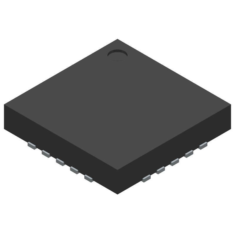
3D Model
Available Download Formats
By downloading CAD models, you agree to our Terms & Conditions and Privacy Policy
18 GHz Microwave PLL Synthesizer
Tip: Data for a part may vary between manufacturers. You can filter for manufacturers on the top of the page next to the part image and part number.
ADF41020BCPZ-RL7 by Analog Devices Inc is a PLL or Frequency Synthesis Circuit.
PLL or Frequency Synthesis Circuits are under the broader part category of Signal Circuits.
A signal is an electronic means of transmitting information, either as an analog signal with continuous values or a digital signal with discrete values. Signals are used in various systems and networks. Read more about Signal Circuits on our Signal Circuits part category page.
| Part # | Distributor | Description | Stock | Price | Buy | |
|---|---|---|---|---|---|---|
|
|
Rochester Electronics | 18 GHz Microwave PLL Synthesizer RoHS: Compliant Status: Obsolete Min Qty: 1 | 104 |
|
$14.6600 / $18.3200 | Buy Now |
|
|
Vyrian | Other Function Semiconductors | 5247 |
|
RFQ | |
|
|
Win Source Electronics | IC CLK/FREQ SYNTH 20LFCSP | 4335 |
|
$42.5588 / $54.9717 | Buy Now |
By downloading CAD models, you agree to our Terms & Conditions and Privacy Policy
|
|
ADF41020BCPZ-RL7
Analog Devices Inc
Buy Now
Datasheet
|
Compare Parts:
ADF41020BCPZ-RL7
Analog Devices Inc
18 GHz Microwave PLL Synthesizer
Select a part to compare: |
| Pbfree Code | No | |
| Rohs Code | Yes | |
| Part Life Cycle Code | Obsolete | |
| Ihs Manufacturer | ANALOG DEVICES INC | |
| Package Description | LFCSP-20 | |
| Pin Count | 20 | |
| Manufacturer Package Code | CP-20-6 | |
| Reach Compliance Code | compliant | |
| ECCN Code | EAR99 | |
| HTS Code | 8542.39.00.01 | |
| Samacsys Manufacturer | Analog Devices | |
| Analog IC - Other Type | PLL FREQUENCY SYNTHESIZER | |
| JESD-30 Code | S-XQCC-N20 | |
| JESD-609 Code | e3 | |
| Length | 4 mm | |
| Moisture Sensitivity Level | 3 | |
| Number of Functions | 1 | |
| Number of Terminals | 20 | |
| Operating Temperature-Max | 85 °C | |
| Operating Temperature-Min | -40 °C | |
| Package Body Material | UNSPECIFIED | |
| Package Code | HVQCCN | |
| Package Equivalence Code | LCC20,.16SQ,20 | |
| Package Shape | SQUARE | |
| Package Style | CHIP CARRIER, HEAT SINK/SLUG, VERY THIN PROFILE | |
| Peak Reflow Temperature (Cel) | 260 | |
| Qualification Status | Not Qualified | |
| Seated Height-Max | 0.8 mm | |
| Supply Current-Max (Isup) | 30 mA | |
| Supply Voltage-Max (Vsup) | 3.15 V | |
| Supply Voltage-Min (Vsup) | 2.85 V | |
| Supply Voltage-Nom (Vsup) | 3 V | |
| Surface Mount | YES | |
| Temperature Grade | INDUSTRIAL | |
| Terminal Finish | Matte Tin (Sn) | |
| Terminal Form | NO LEAD | |
| Terminal Pitch | 0.5 mm | |
| Terminal Position | QUAD | |
| Time@Peak Reflow Temperature-Max (s) | 30 | |
| Width | 4 mm |
This table gives cross-reference parts and alternative options found for ADF41020BCPZ-RL7. The Form Fit Function (FFF) tab will give you the options that are more likely to serve as direct pin-to-pin alternates or drop-in parts. The Functional Equivalents tab will give you options that are likely to match the same function of ADF41020BCPZ-RL7, but it may not fit your design. Always verify details of parts you are evaluating, as these parts are offered as suggestions for what you are looking for and are not guaranteed.
| Part Number | Manufacturer | Composite Price | Description | Compare |
|---|---|---|---|---|
| ADF41513BCPZ | Analog Devices Inc | $48.4587 | 26.5 GHz, Integer N/Fractional-N, PLL Synthesizer | ADF41020BCPZ-RL7 vs ADF41513BCPZ |
A 4-layer PCB with a solid ground plane and a separate power plane is recommended. Keep the signal traces short and away from the power planes. Use a common mode filter or a pi-filter to reduce noise and EMI.
Use a low-ESR capacitor (e.g., 100nF) between VDD and GND, and a 10uF capacitor between AVDD and AGND. Ensure the power supply is clean and regulated, and use a voltage regulator if necessary.
The maximum frequency deviation is dependent on the PLL loop bandwidth and the modulation frequency. Typically, it's around ±10MHz to ±20MHz, but it can be optimized by adjusting the PLL loop filter components and the modulation frequency.
Use the PLL loop filter design tool provided by Analog Devices or a third-party tool to optimize the filter components (R1, R2, C1, C2) based on the desired loop bandwidth, phase margin, and settling time.
Use a 3-wire serial interface (SPI) to program the device. Ensure the clock frequency is within the recommended range (10kHz to 1MHz), and use a pull-up resistor on the SCLK line to prevent clock stretching.