-
Part Symbol
-
Footprint
-
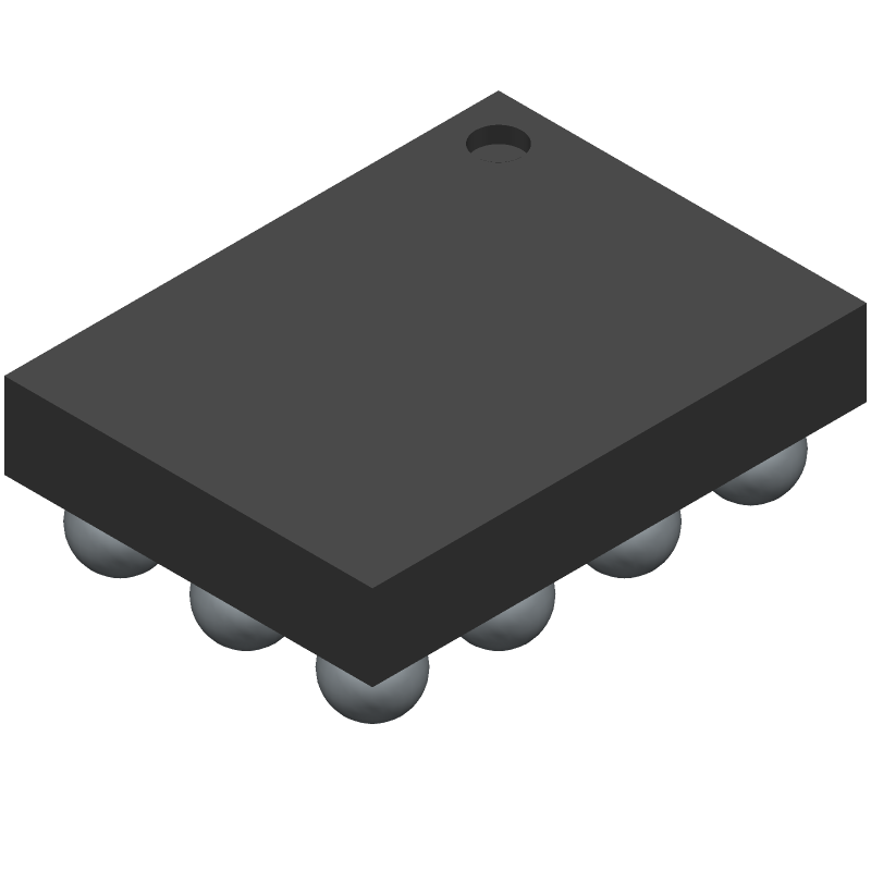
3D Model
Available Download Formats
By downloading CAD models, you agree to our Terms & Conditions and Privacy Policy
5 V Charge Pump HDMI Tx Companion Chip
Tip: Data for a part may vary between manufacturers. You can filter for manufacturers on the top of the page next to the part image and part number.
| Part # | Distributor | Description | Stock | Price | Buy | |
|---|---|---|---|---|---|---|
|
|
Rochester Electronics | 5 V Charge Pump Hdmi Tx Companion Chip RoHS: Compliant Status: End of Life / Last Time Buy Min Qty: 1 | 21000 |
|
$1.1700 / $1.4600 | Buy Now |
By downloading CAD models, you agree to our Terms & Conditions and Privacy Policy
|
|
AD9394BCBZ-R7
Analog Devices Inc
Buy Now
Datasheet
|
Compare Parts:
AD9394BCBZ-R7
Analog Devices Inc
5 V Charge Pump HDMI Tx Companion Chip
Select a part to compare: |
| Pbfree Code | No | |
| Rohs Code | Yes | |
| Part Life Cycle Code | Obsolete | |
| Ihs Manufacturer | ANALOG DEVICES INC | |
| Part Package Code | BGA | |
| Package Description | 2 X 1.50 MM, ROHS COMPLIANT, WLCSP-12 | |
| Pin Count | 12 | |
| Reach Compliance Code | compliant | |
| ECCN Code | EAR99 | |
| HTS Code | 8542.39.00.01 | |
| Samacsys Manufacturer | Analog Devices | |
| Consumer IC Type | CONSUMER CIRCUIT | |
| JESD-30 Code | R-PBGA-B12 | |
| Length | 1.96 mm | |
| Moisture Sensitivity Level | 1 | |
| Number of Functions | 1 | |
| Number of Terminals | 12 | |
| Operating Temperature-Max | 85 °C | |
| Operating Temperature-Min | -40 °C | |
| Package Body Material | PLASTIC/EPOXY | |
| Package Code | VFBGA | |
| Package Equivalence Code | BGA12,3X4,20 | |
| Package Shape | RECTANGULAR | |
| Package Style | GRID ARRAY | |
| Peak Reflow Temperature (Cel) | 260 | |
| Qualification Status | Not Qualified | |
| Seated Height-Max | 0.66 mm | |
| Supply Voltage-Max (Vsup) | 4.5 V | |
| Supply Voltage-Min (Vsup) | 2.5 V | |
| Surface Mount | YES | |
| Technology | CMOS | |
| Temperature Grade | INDUSTRIAL | |
| Terminal Form | BALL | |
| Terminal Pitch | 0.5 mm | |
| Terminal Position | BOTTOM | |
| Time@Peak Reflow Temperature-Max (s) | 30 | |
| Width | 1.46 mm |
A good PCB layout is crucial for the AD9394BCBZ-R7. It's recommended to follow the layout guidelines provided in the datasheet, including keeping the analog and digital grounds separate, using a solid ground plane, and minimizing noise coupling between the analog and digital sections.
The AD9394BCBZ-R7 requires calibration for optimal performance. It's recommended to follow the calibration procedure outlined in the datasheet, which includes setting the internal voltage reference, adjusting the gain and offset, and performing a system calibration to ensure accurate measurements.
The maximum clock frequency for the AD9394BCBZ-R7 is 100 MHz. However, the actual clock frequency used may be limited by the specific application and the performance requirements of the system.
The AD9394BCBZ-R7 is a high-performance device that can generate heat during operation. It's recommended to provide adequate thermal management, such as using a heat sink or thermal pad, to ensure the device operates within its specified temperature range.
Proper power supply decoupling is essential for the AD9394BCBZ-R7. It's recommended to use a combination of ceramic and electrolytic capacitors to decouple the power supply, with a minimum of 0.1 μF and 10 μF capacitors, respectively, placed close to the device.