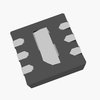
Part Details for 74LVC1G80GS by NXP Semiconductors
Overview of 74LVC1G80GS by NXP Semiconductors
- Distributor Offerings: (0 listings)
- Number of FFF Equivalents: (0 replacements)
- CAD Models: (Request Part)
- Number of Functional Equivalents: (0 options)
- Part Data Attributes: (Available)
- Reference Designs: (Not Available)
Tip: Data for a part may vary between manufacturers. You can filter for manufacturers on the top of the page next to the part image and part number.
Applications
Education and Research
Industrial Automation
Financial Technology (Fintech)
Healthcare
Electronic Manufacturing
Part Details for 74LVC1G80GS
74LVC1G80GS CAD Models
74LVC1G80GS Part Data Attributes
|
|
74LVC1G80GS
NXP Semiconductors
Buy Now
Datasheet
|
Compare Parts:
74LVC1G80GS
NXP Semiconductors
LVC/LCX/Z SERIES, POSITIVE EDGE TRIGGERED D FLIP-FLOP, INVERTED OUTPUT, PDSO6, 1 X 1 MM, 0.35 MM HEIGHT, 0.35 MM PITCH, SOT-1202, SON-6
|
| Rohs Code | Yes | |
| Part Life Cycle Code | Transferred | |
| Ihs Manufacturer | NXP SEMICONDUCTORS | |
| Part Package Code | SON | |
| Package Description | 1 X 1 MM, 0.35 MM HEIGHT, 0.35 MM PITCH, SOT-1202, SON-6 | |
| Pin Count | 6 | |
| Reach Compliance Code | unknown | |
| HTS Code | 8542.39.00.01 | |
| Family | LVC/LCX/Z | |
| JESD-30 Code | S-PDSO-N6 | |
| JESD-609 Code | e3 | |
| Length | 1 mm | |
| Logic IC Type | D FLIP-FLOP | |
| Moisture Sensitivity Level | 1 | |
| Number of Functions | 1 | |
| Number of Terminals | 6 | |
| Operating Temperature-Max | 125 °C | |
| Operating Temperature-Min | -40 °C | |
| Output Polarity | INVERTED | |
| Package Body Material | PLASTIC/EPOXY | |
| Package Code | VSON | |
| Package Shape | SQUARE | |
| Package Style | SMALL OUTLINE, VERY THIN PROFILE | |
| Peak Reflow Temperature (Cel) | NOT SPECIFIED | |
| Propagation Delay (tpd) | 13 ns | |
| Qualification Status | Not Qualified | |
| Seated Height-Max | 0.35 mm | |
| Supply Voltage-Max (Vsup) | 5.5 V | |
| Supply Voltage-Min (Vsup) | 1.65 V | |
| Supply Voltage-Nom (Vsup) | 3.3 V | |
| Surface Mount | YES | |
| Technology | CMOS | |
| Temperature Grade | AUTOMOTIVE | |
| Terminal Finish | Tin (Sn) | |
| Terminal Form | NO LEAD | |
| Terminal Pitch | 0.35 mm | |
| Terminal Position | DUAL | |
| Time@Peak Reflow Temperature-Max (s) | NOT SPECIFIED | |
| Trigger Type | POSITIVE EDGE | |
| Width | 1 mm | |
| fmax-Min | 200 MHz |
