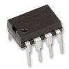
Part Details for 1B21AN by Analog Devices Inc
Results Overview of 1B21AN by Analog Devices Inc
- Distributor Offerings: (0 listings)
- Number of FFF Equivalents: (0 replacements)
- CAD Models: (Request Part)
- Number of Functional Equivalents: (0 options)
- Part Data Attributes: (Available)
- Reference Designs: (Not Available)
Tip: Data for a part may vary between manufacturers. You can filter for manufacturers on the top of the page next to the part image and part number.
1B21AN Information
1B21AN by Analog Devices Inc is an Other Signal Circuit.
Other Signal Circuits are under the broader part category of Signal Circuits.
A signal is an electronic means of transmitting information, either as an analog signal with continuous values or a digital signal with discrete values. Signals are used in various systems and networks. Read more about Signal Circuits on our Signal Circuits part category page.
Part Details for 1B21AN
1B21AN CAD Models
1B21AN Part Data Attributes
|
|
1B21AN
Analog Devices Inc
Buy Now
Datasheet
|
Compare Parts:
1B21AN
Analog Devices Inc
Isolated, Loop-Powered Voltage-to-Current Converter
Select a part to compare: |
| Pbfree Code | No | |
| Rohs Code | No | |
| Part Life Cycle Code | Obsolete | |
| Ihs Manufacturer | ANALOG DEVICES INC | |
| Part Package Code | DIP | |
| Package Description | DIP-38/8 | |
| Pin Count | 8 | |
| Reach Compliance Code | not_compliant | |
| ECCN Code | EAR99 | |
| HTS Code | 9033.00.90.00 | |
| Analog IC - Other Type | ANALOG CIRCUIT | |
| JESD-30 Code | R-PDIP-T8 | |
| Neg Supply Voltage-Max (Vsup) | -15.75 V | |
| Neg Supply Voltage-Min (Vsup) | -14.25 V | |
| Neg Supply Voltage-Nom (Vsup) | -15 V | |
| Number of Functions | 1 | |
| Number of Terminals | 8 | |
| Operating Temperature-Max | 85 °C | |
| Operating Temperature-Min | -25 °C | |
| Package Body Material | PLASTIC/EPOXY | |
| Package Code | DIP | |
| Package Equivalence Code | DIP8/38,.5 | |
| Package Shape | RECTANGULAR | |
| Package Style | IN-LINE | |
| Peak Reflow Temperature (Cel) | NOT SPECIFIED | |
| Qualification Status | Not Qualified | |
| Seated Height-Max | 8.9 mm | |
| Supply Current-Max (Isup) | 10 mA | |
| Supply Voltage-Max (Vsup) | 15.75 V | |
| Supply Voltage-Min (Vsup) | 14.25 V | |
| Supply Voltage-Nom (Vsup) | 15 V | |
| Surface Mount | NO | |
| Technology | HYBRID | |
| Temperature Grade | OTHER | |
| Terminal Form | THROUGH-HOLE | |
| Terminal Pitch | 2.54 mm | |
| Terminal Position | DUAL | |
| Time@Peak Reflow Temperature-Max (s) | NOT SPECIFIED | |
| Width | 17.78 mm |
1B21AN Frequently Asked Questions (FAQ)
-
A good PCB layout for the 1B21AN involves keeping the input and output traces short and separate, using a solid ground plane, and placing decoupling capacitors close to the device. A 4-layer PCB with a dedicated power plane and a solid ground plane is recommended.
-
To ensure proper biasing, connect the VCC pin to a stable voltage source, and decouple it with a 0.1uF capacitor to ground. The input common-mode voltage should be set to VCC/2, and the output should be terminated with a 50Ω load to ensure maximum bandwidth.
-
The 1B21AN is rated for operation from -40°C to +85°C. However, it's recommended to derate the device's performance at higher temperatures to ensure reliability and prevent thermal shutdown.
-
To minimize EMI, use a shielded enclosure, keep the device away from high-frequency sources, and use a common-mode choke or ferrite bead on the input and output lines. Additionally, ensure good PCB layout practices, such as keeping traces short and using a solid ground plane.
-
The 1B21AN requires a 50Ω input termination to ensure maximum bandwidth and minimize reflections. The output should also be terminated with a 50Ω load to ensure proper signal integrity.
